

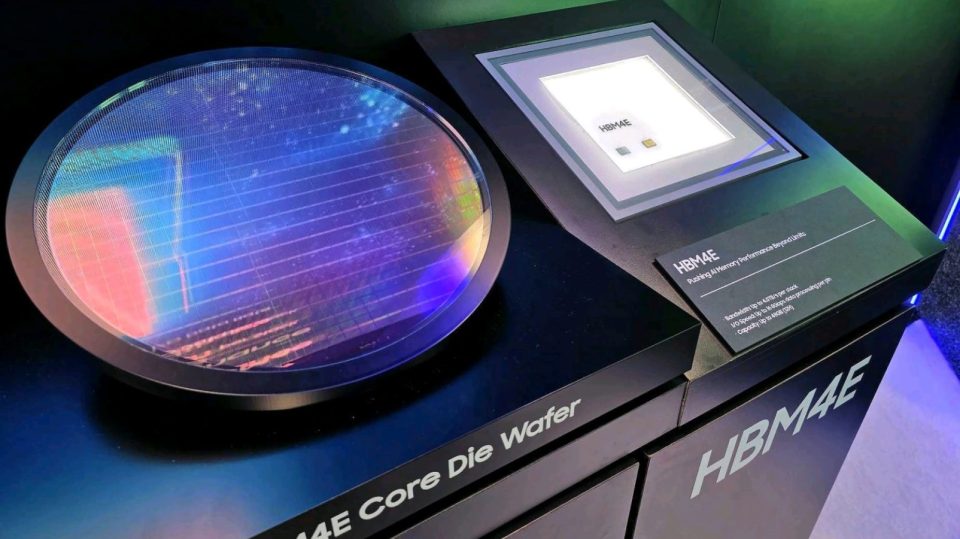
Samsung says it has applied its 2 nm process to upcoming HBM5 modules, targeting a roughly 50% performance increase over the previous generation. The company attributes the gain to using 2 nm on the “base die” — the tier that supports the stacked DRAM dies — and to a higher density of vertical interconnects between layers.
HBM5 and the impact of 2 nm
According to Gu Jahum, head of technology development for Samsung’s foundry division, HBM5 will handle data more than 50% faster than HBM4E. That improvement is credited to integrating the 2 nm node at the base-die level, a move intended to boost both bandwidth and power efficiency of the memory modules.
Tighter TSV pitch and stacked architecture
Samsung also says HBM5 will employ through-silicon vias (TSVs) with a tighter pitch. These microscopic vertical electrodes, which connect the stacked DRAM layers, increase effective bandwidth between dies and optimize intra-package communication.
Where HBM4 sits on the roadmap
The company adds that its 2 nm Gate-All-Around (GAA) technology will be used for HBM4. This distinction highlights that 2 nm will be deployed differently across HBM product families and reflects a planned evolution of process technology across HBM generations.
What this means for AI infrastructure
The disclosures underscore Samsung’s push on high-bandwidth memory — a critical component for AI accelerators and modern data centers. By applying 2 nm to the base die and densifying TSVs, Samsung aims to meet growing demands for throughput and energy efficiency in next‑generation compute platforms.
