

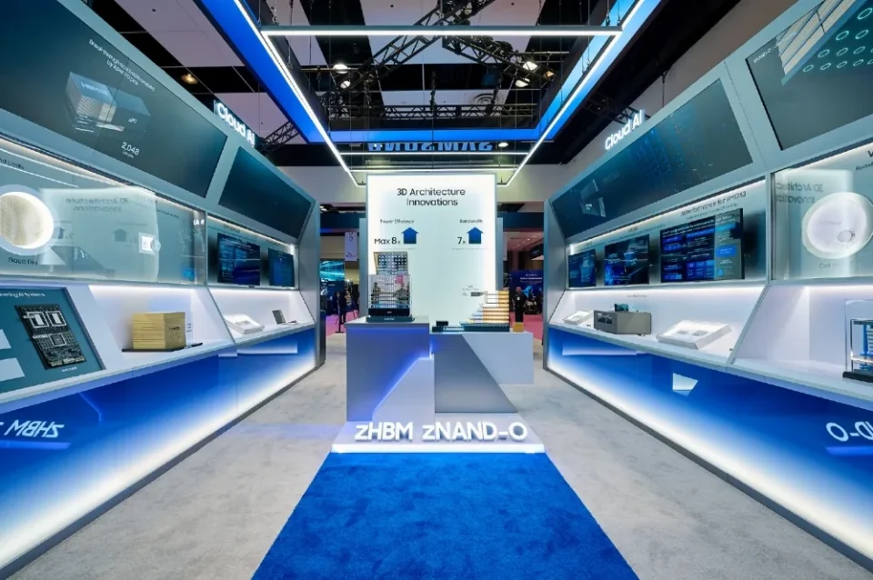
Samsung Electronics unveiled zHBM, a new memory chip concept for future AI servers and data centers, at the Future of Memory and Storage (FMS) 2026 expo in Santa Clara, California. The company claims zHBM can deliver approximately eight times (8x) higher data-transfer speeds and more than 10 times (10x) the memory density of HBM5 chips, which have not yet launched.
How zHBM achieves higher speed and density
The concept stacks HBM chips directly on top of an AI accelerator rather than placing them horizontally beside it on an interposer, shortening the distance between processor and memory and which Samsung says could improve data-transfer speeds. Samsung also attributes the projected increase in memory density to next-generation wafer-bonding technology that would enable the roughly 10x density gain over HBM5.
Potential benefits for AI servers
Samsung claims zHBM could offer three times better energy efficiency and 50% lower thermal resistance than conventional memory configurations. The company says zHBM chips could support customer-specific designs, allowing customized components to be integrated into the layer between the AI accelerator and the memory chip to enable even higher memory capacity and improve accelerator performance.
Samsung Electronics’ zHBM concept was explained by a Samsung executive at the Future Memory And Storage 2026 expo in Santa Clara, California.
