

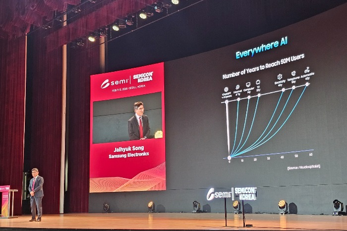
Samsung will postpone the full-scale commercial deployment of High-NA EUV lithography until its 1nm process node (A10), with chips from that node expected to begin shipping around 2030, Park Chang-min of Samsung’s Semiconductor R&D Center said at the Next Generation Lithography + Patterning Conference (NGL 2026) (via @Jukan05).
Why Samsung is postponing High-NA EUV
The company had initially planned to use High-NA EUV equipment for its 2nm and 1.4nm nodes but found the supporting ecosystem immature. Essential components — including masks, pellicles and specialized materials needed to fully exploit High-NA machines — are still lacking and require further joint development. Each High-NA EUV machine is estimated to cost between $350 million and $400 million, making the equipment extremely expensive even for leading foundries like Samsung.
Short-term roadmap: 2nm and 1.4nm without High-NA
Samsung Foundry now plans to rely on standard 0.33 NA EUV equipment combined with multi-patterning techniques for its next-generation 2nm and 1.4nm process nodes, rather than deploying High-NA systems at those nodes.
What High-NA EUV brings
High-NA EUV increases the numerical aperture from 0.33 to 0.55, gathering more light to improve resolution. That capability enables single-patterning of ultra-fine circuits, reduces production steps and improves design flexibility.
Samsung was one of the first companies to launch chips produced on a 3nm-class node; the new schedule places full commercial use of High-NA EUV at the later 1nm (A10) milestone.
