

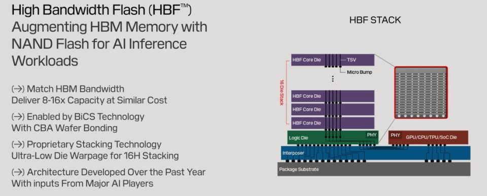
High Bandwidth Flash (HBF), introduced jointly by SK hynix and SanDisk, aims to bridge the performance gap between High Bandwidth Memory (HBM) and SSDs for AI inference by offering configurations up to 512GB and bandwidths ranging from 0.4TB/s to 3TB/s.
High Bandwidth Flash: architecture, capacity and role
HBF positions itself between HBM and enterprise SSDs: it uses multiple stacked memory dies like HBM but relies on NAND flash instead of DRAM to increase storage capacity. The HBF specifications allow stacking NAND dies in eight or 16 layers and support single configurations up to 512GB, with bandwidths from 0.4TB/s to 3TB/s. Its intended role is to complement HBM’s limited capacity rather than replace it. For example, the firms note that an AI model with 500 billion parameters would require roughly 500GB if one gigabyte stores one billion parameters, making full HBM storage impractical and HBF a more economical option for holding large models used in inference.
Ecosystem connectivity and industry context
HBF also supports the UCIe (Universal Chiplet Interconnect Express) specification, allowing it to connect to various CPUs and GPUs and adding a layer of flexibility across system architectures. Kim Chun-sung, head of solution development at SK hynix, said the company “will expand the boundaries between memory and storage and contribute to building new architectures that enhance overall system efficiency.”
Meanwhile, Samsung is pursuing a parallel approach by developing and mass-producing CMX solutions and manufacturing V10 and V11 NAND flash with up to 500 stacked layers. Samsung’s efforts target ultra-fast storage for AI servers that seek quicker data access to increase GPU offloading and improve AI inference. Which standard will pick up the pace? It looks like we’ll find out in the coming months.
